- 您现在的位置:买卖IC网 > Sheet目录480 > MTD5P06VT4 (ON Semiconductor)MOSFET P-CH 60V 5A DPAK
�� �
�
�MTD5P06V�
�Preferred� Device�
�Power� MOSFET�
�5� Amps,� 60� Volts� P?Channel� DPAK�
�This� Power� MOSFET� is� designed� to� withstand� high� energy� in� the�
�avalanche� and� commutation� modes.� Designed� for� low� voltage,� high�
�speed� switching� applications� in� power� supplies,� converters� and� power�
�motor� controls,� these� devices� are� particularly� well� suited� for� bridge�
�circuits� where� diode� speed� and� commutating� safe� operating� areas� are�
�http://onsemi.com�
�critical� and� offer� additional� safety� margin� against� unexpected� voltage�
�transients.�
�Features�
�?� Avalanche� Energy� Specified�
�?� I� DSS� and� V� DS(on)� Specified� at� Elevated� Temperature�
�?� Pb?Free� Packages� are� Available�
�V� (BR)DSS�
�60� V�
�R� DS(on)� TYP�
�340� m� W�
�P?Channel�
�D�
�I� D� MAX�
�5.0� A�
�MAXIMUM� RATINGS� (T� C� =� 25� °� C� unless� otherwise� noted)�
�Rating�
�Drain?to?Source� Voltage�
�Drain?to?Gate� Voltage� (R� GS� =� 1.0� M� W� )�
�Gate?to?Source� Voltage�
�?� Continuous�
�?� Non?repetitive� (t� p� ≤� 10� ms)�
�Symbol�
�V� DSS�
�V� DGR�
�V� GS�
�V� GSM�
�Value�
�60�
�60�
�±� 15�
�±� 25�
�Unit�
�Vdc�
�Vdc�
�Vdc�
�Vpk�
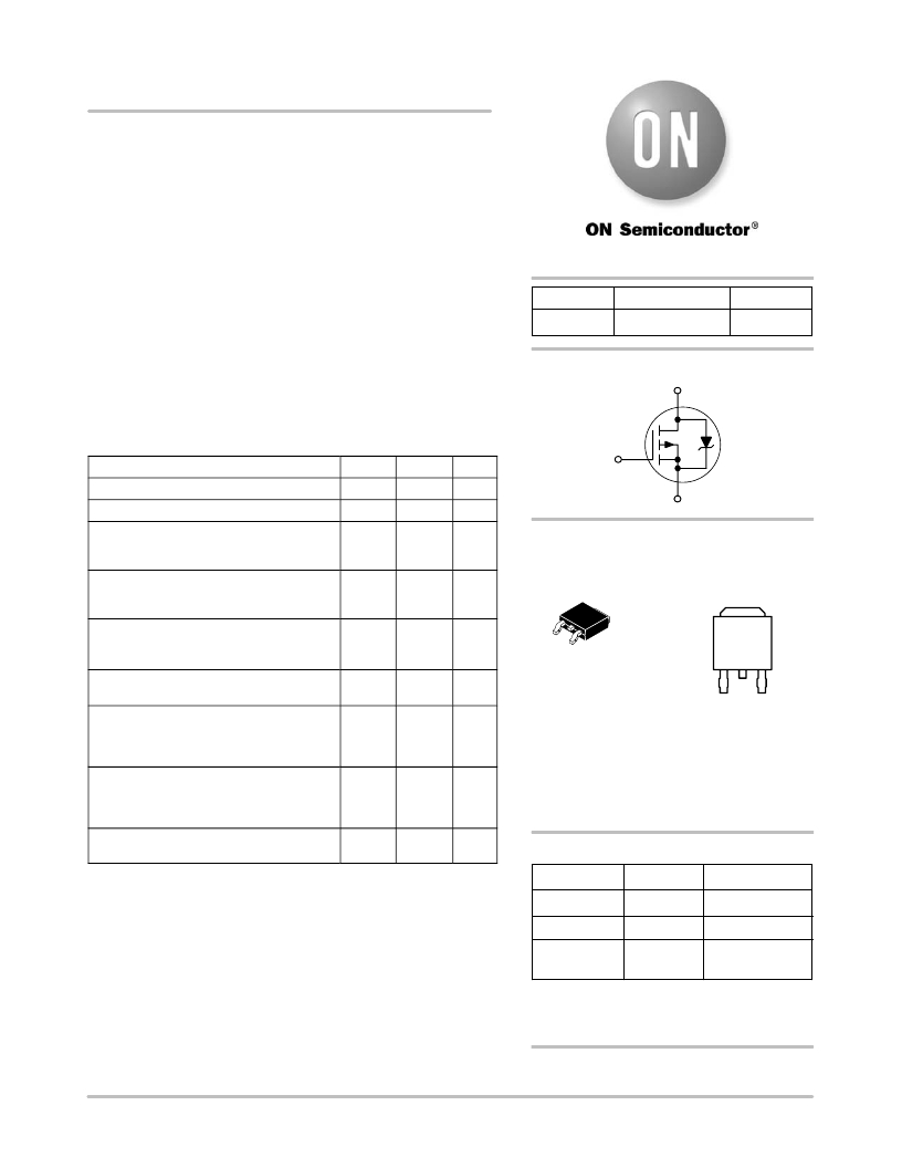
�G�
�S�
�MARKING�
�DIAGRAM�
�Drain� Current� ?� Continuous� @� 25� °� C�
�?� Continuous� @� 100� °� C�
�?� Single� Pulse� (t� p� ≤� 10� m� s)�
�I� D�
�I� D�
�I� DM�
�5�
�4�
�18�
�Adc�
�Apk�
�4�
�4�
�Drain�
�Total� Power� Dissipation� @� 25� °� C�
�Derate� above� 25� °� C�
�Total� Power� Dissipation� @� T� A� =� 25� °� C� (Note� 2)�
�P� D�
�40�
�0.27�
�2.1�
�W�
�W/� °� C�
�W�
�1� 2�
�3�
�DPAK�
�CASE� 369C�
�STYLE� 2�
�Operating� and� Storage� Temperature� Range�
�Single� Pulse� Drain?to?Source� Avalanche�
�Energy� ?� Starting� T� J� =� 25� °� C�
�T� J� ,� T� stg�
�E� AS�
�?55� to�
�175�
�125�
�°� C�
�mJ�
�1�
�Gate�
�2�
�Drain�
�3�
�Source�
�(V� DD� =� 25� Vdc,� V� GS� =� 10� Vdc,� Peak�
�I� L� =� 5� Apk,� L� =� 10� mH,� R� G� =� 25� W� )�
�Y�
�=� Year�
�Thermal� Resistance�
�°� C/W�
�WW�
�=� Work� Week�
�Junction?to?Case�
�Junction?to?Ambient� (Note� 1)�
�Junction?to?Ambient� (Note� 2)�
�R� q� JC�
�R� q� JA�
�R� q� JA�
�3.75�
�100�
�71.4�
�5P06V�
�G�
�=� Device� Code�
�=� Pb?Free� Package�
�Maximum� Lead� Temperature� for� Soldering�
�Purposes,� 1/8� ″� from� Case� for� 10� seconds�
�T� L�
�260�
�°� C�
�ORDERING� INFORMATION�
�Stresses� exceeding� Maximum� Ratings� may� damage� the� device.� Maximum�
�Ratings� are� stress� ratings� only.� Functional� operation� above� the� Recommended�
�Operating� Conditions� is� not� implied.� Extended� exposure� to� stresses� above� the�
�Recommended� Operating� Conditions� may� affect� device� reliability.�
�1.� When� surface� mounted� to� an� FR4� board� using� the� minimum� recommended�
�pad� size.�
�2.� When� surface� mounted� to� an� FR?4� board� using� the� 0.5� sq� in� drain� pad� size.�
�Device�
�MTD5P06V�
�MTD5P06VT4�
�MTD5P06VT4G�
�Package�
�DPAK�
�DPAK�
�DPAK�
�Shipping� ?�
�75� Units/Rail�
�2500/Tape� &� Reel�
�2500/Tape� &� Reel�
�(Pb?Free)�
�?For� information� on� tape� and� reel� specifications,�
�including� part� orientation� and� tape� sizes,� please�
�refer� to� our� Tape� and� Reel� Packaging� Specifications�
�Brochure,� BRD8011/D.�
�Preferred� devices� are� recommended� choices� for� future� use�
�and� best� overall� value.�
�?� Semiconductor� Components� Industries,� LLC,� 2006�
�July,� 2006� ?� Rev.� 6�
�1�
�Publication� Order� Number:�
�MTD5P06V/D�
�发布紧急采购,3分钟左右您将得到回复。
相关PDF资料
MTD6000PT-T
PHOTOTRANS 880NM PIGTAIL DOME
MTD6100PT
PHOTO DIODE 880NM DOME CLR
MTD6N15T4
MOSFET N-CH 150V 6A DPAK
MTD6N20ET4
MOSFET N-CH 200V 6A DPAK
MTD6P10E
MOSFET P-CH 100V 6A DPAK
MTD8000N4-T
PHOTOTRANS 880NM DOME CLR TO-18
MTD8600N-T
PHOTOTRANS 880NM DOME CLR TO-18
MTD8600N4-T
PHOTOTRANS 880NM DOME CLR TO-18
相关代理商/技术参数
MTD5P06VT4G
功能描述:MOSFET PFET DPAK 60V 5A 450mOhm RoHS:否 制造商:STMicroelectronics 晶体管极性:N-Channel 汲极/源极击穿电压:650 V 闸/源击穿电压:25 V 漏极连续电流:130 A 电阻汲极/源极 RDS(导通):0.014 Ohms 配置:Single 最大工作温度: 安装风格:Through Hole 封装 / 箱体:Max247 封装:Tube
MTD5P06VT4G
制造商:ON Semiconductor 功能描述:MOSFET
MTD5P06VT4GV
功能描述:MOSFET Single P-Ch 60V 5A RoHS:否 制造商:STMicroelectronics 晶体管极性:N-Channel 汲极/源极击穿电压:650 V 闸/源击穿电压:25 V 漏极连续电流:130 A 电阻汲极/源极 RDS(导通):0.014 Ohms 配置:Single 最大工作温度: 安装风格:Through Hole 封装 / 箱体:Max247 封装:Tube
MTD6000PT
制造商:MARKTECH 制造商全称:Marktech Corporate 功能描述:Photo Transistor
MTD6000PTT
制造商:MARKTECH 制造商全称:Marktech Corporate 功能描述:Peak Sensitivity Wavelength: 880nm
MTD6000PT-T
功能描述:PHOTOTRANS 880NM PIGTAIL DOME RoHS:是 类别:传感器,转换器 >> 光学 - 光电检测器 - 光电晶体管 系列:- 标准包装:1,200 系列:- 电压 - 集电极发射极击穿(最大):30V 电流 - 集电极 (Ic)(最大):1mA 电流 - 暗 (Id)(最大):100nA 波长:880nm 视角:24° 功率 - 最大:100mW 安装类型:通孔 方向:顶视图 封装/外壳:径向
MTD6000PT-T-DIG
制造商:Marktech Optoelectronics 功能描述:PHOTOTRANS 880NM PIGTAIL DOME
MTD6010A
制造商:MARKTECH 制造商全称:Marktech Corporate 功能描述:PHOTO TRANSISTOR